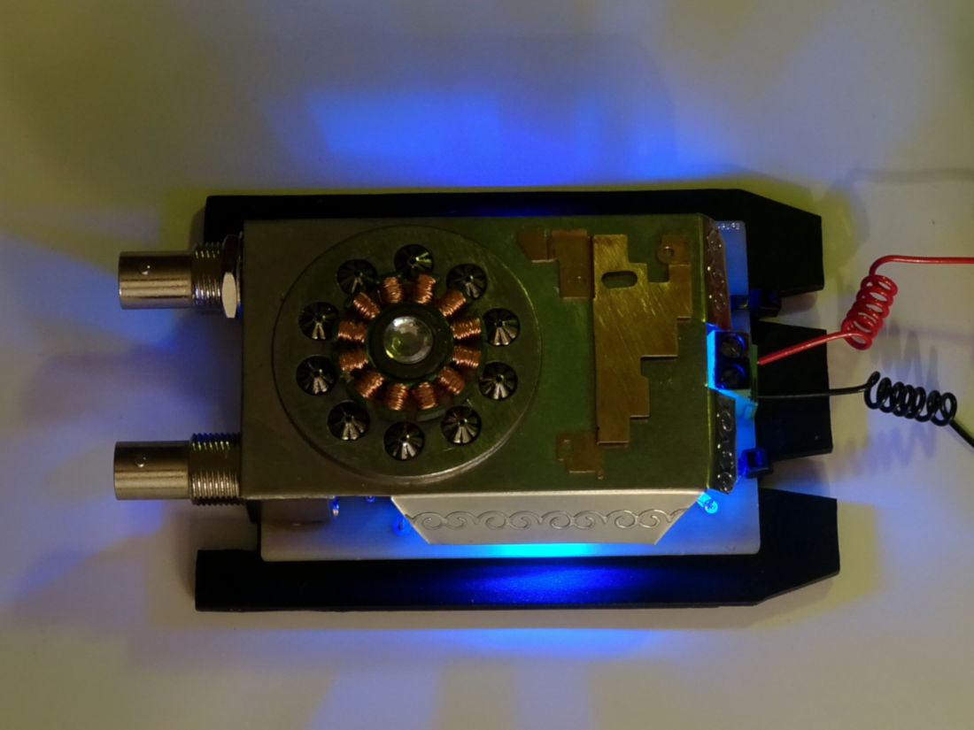
Electro-mechanical details
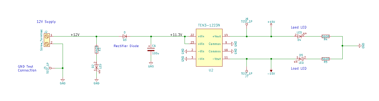
Power schematic.
Notice the load LEDs. They are not just pretty, but needed to introduce a load to the DC-DC converter as these are only specified with a 1% voltage accuracy when loaded at 10% - 100% of full capacity. The entropy source and buffer op-amps (TL082) require nowhere near this, and so the supply rails would be unpredictable.
And speaking of buffers and such, the schematic below shows the heart of the Zenerglass:-
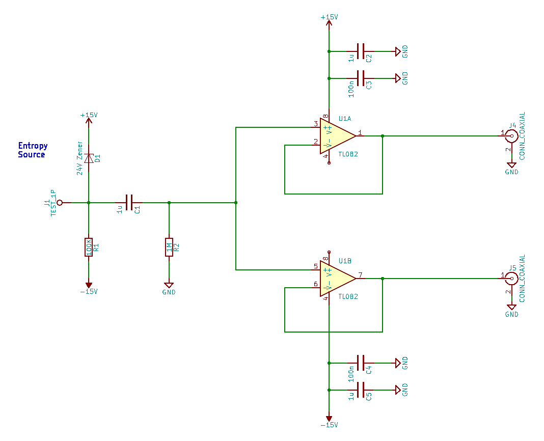
The 24V entropy source, and twin output buffering.
24V Zener D1 is the entropy source operating at 60μA. It’s worth noting that as this diode is encapsulated within transparent glass, it has to be shielded from light with heat shrink tubing. Otherwise incident light would diminish the Zener voltage signal. The signal is then decoupled by C1 and then buffered with no gain by the op-amps to produce twin stiff outputs. Capacitors C2 thru C5 just provide power rail by-passing. R2 is necessary for handling op-amp bias currents. It can be as high as 1MΩ as the TL082 has very high input impedances, being a JFET input type. It should be as high as possible to avoid forming a significant voltage divider with the upstream entropy source (D1, R1) impedance.
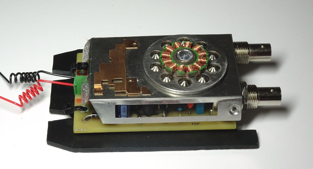
You can see the all important Zener diode (D1) in the middle of the PCB:-
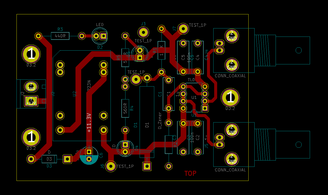
Unremarkable through hole PCB layout.
Complete entropy module.