Electro-mechanical details
Principal components
The Null Gamma Device is based around a 1.4 GHz 64-bit quad-core Raspberry Pi 3 Model B+ single board computer. The entropy source at it’s heart (the Null source) is the cumulation of various quantum and electrical effects on photo sensors within a blacked out 8 Mbit camera operating at ISO 800. The higher the ISO setting, the higher the entropy rate. The device’s Linux (Raspian) operating system is hosted on a 120 GB SSD drive for reliability and longevity.
Entropy generation is essentially the same process as within the Photonic Instrument, other than there being no photon noise as the camera operates in complete darkness.
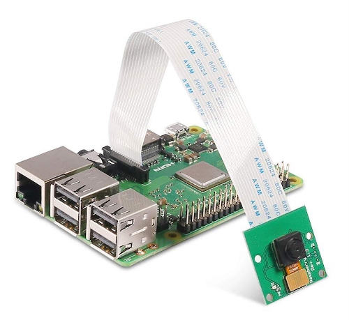
Basic hardware components (stock photo).
SSD drive hosting the Raspian/Linux operating system (stock photo).
Test assembly
The image below is an initial test assembly of the principal components. You can see the Null source on the right hand side, next to the photon shield (black protective enclosure and secondary light barrier). The SSD drive is beneath the Pi, connected via a SATA to USB adapter cable.
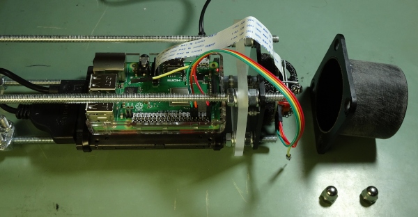
Test assembly of the Null Gamma Device.
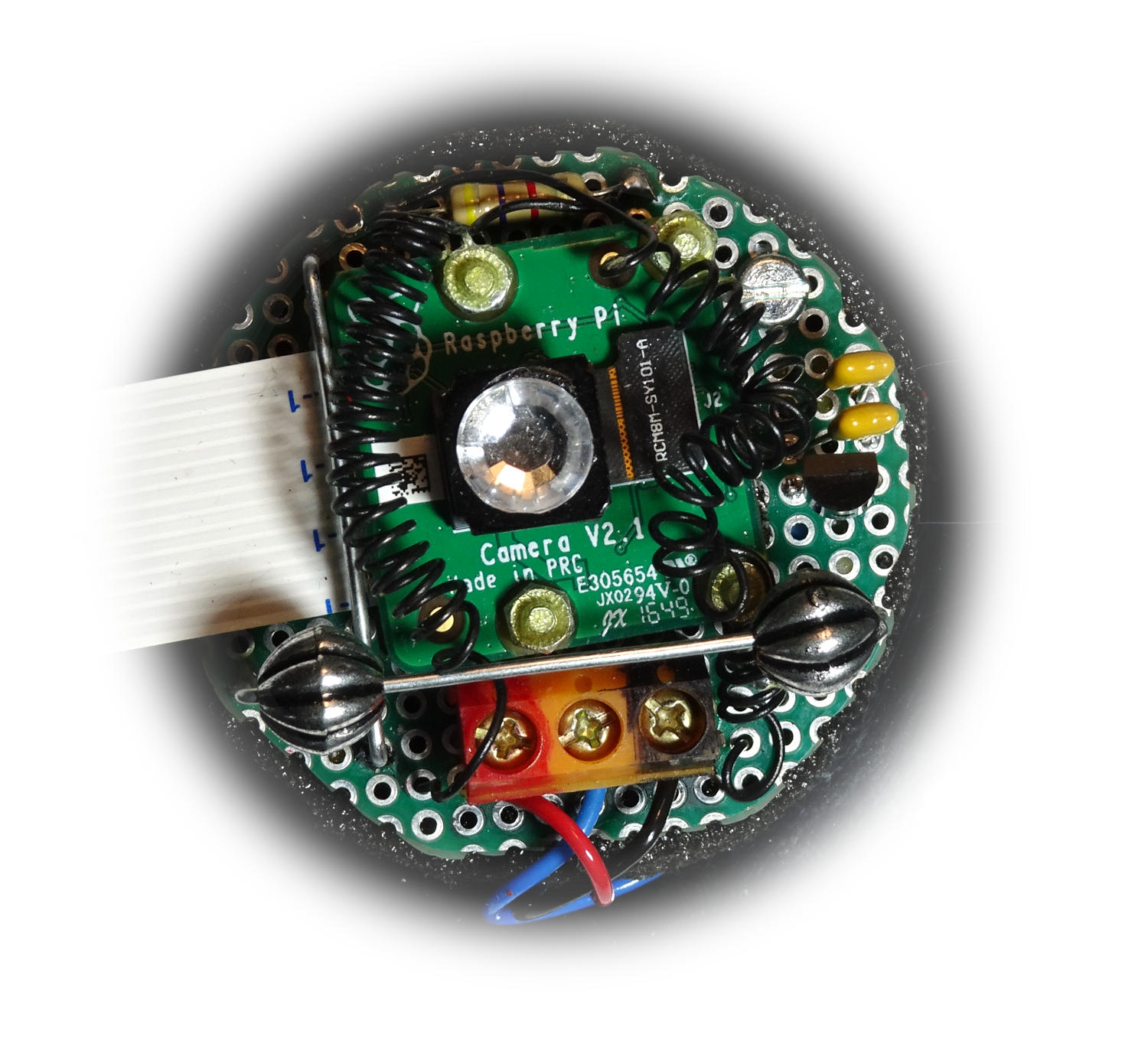
Null source
The CMOS camera is the Null source. The camera is obscured simply by super-glueing a 1.6 mm thick opaque plastic square directly onto the lens mount (having removed the lens itself). It is beneath the central focusing crystal. The camera has been successfully tested for light tightness. Zero light ✔
There is also a DS18B20 digital thermometer adjacent to the camera for temperature monitoring (at the 3 o’clock position below). It is bypassed with two 100 nF ceramic capacitors for good luck. This allows us to assess the relationship between the Null source’s entropy rate and it’s operating temperature.
The Null entropy source. Photon shield removed.
The Null entropy source. Photon shield removed.
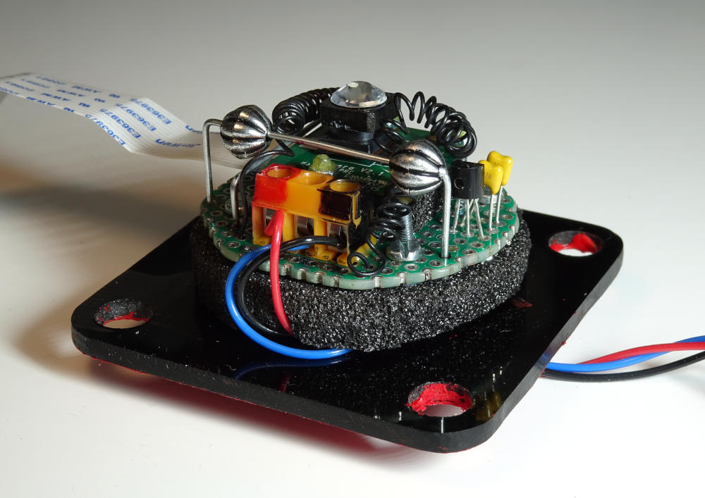
The entire source is encased within a secondary photon shield for security and additional light exclusion. You will be able to notice a thin brown gasket between the top and bottom parts of the photon shield. It improves the light seal, but more importantly allows for the thickness of the camera cable. LED activity indicators are mounted atop the shield that glow alternately red and green every time Null Gamma is accessed.
The Null entropy source encased inside the photon shield, and activity indicators.
I/O PCB
All wiring connections are made via a custom I/O PCB. The PCB and screw connectors are a little more reliable than jumpers and headers. It also holds the pull down circuits for the activity indicators, thermometer peripherals, on/off indicator and supplemental capacitance for the RPi itself. The particular shape does not obstruct air from circulating over the Broadcom chip’s heat spreader.
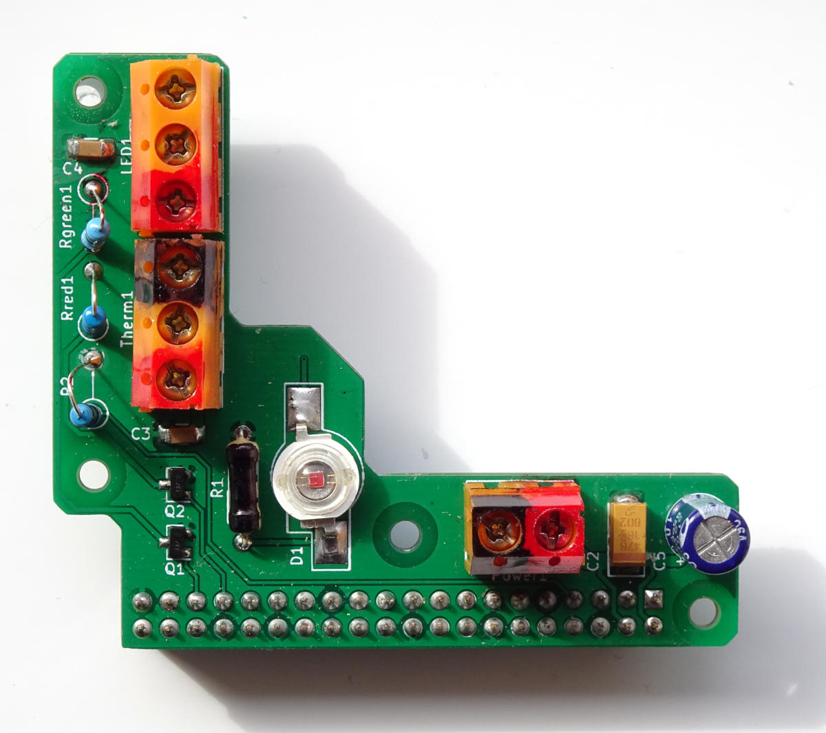
I/O board for wire connections to the Null Gamma RPi.
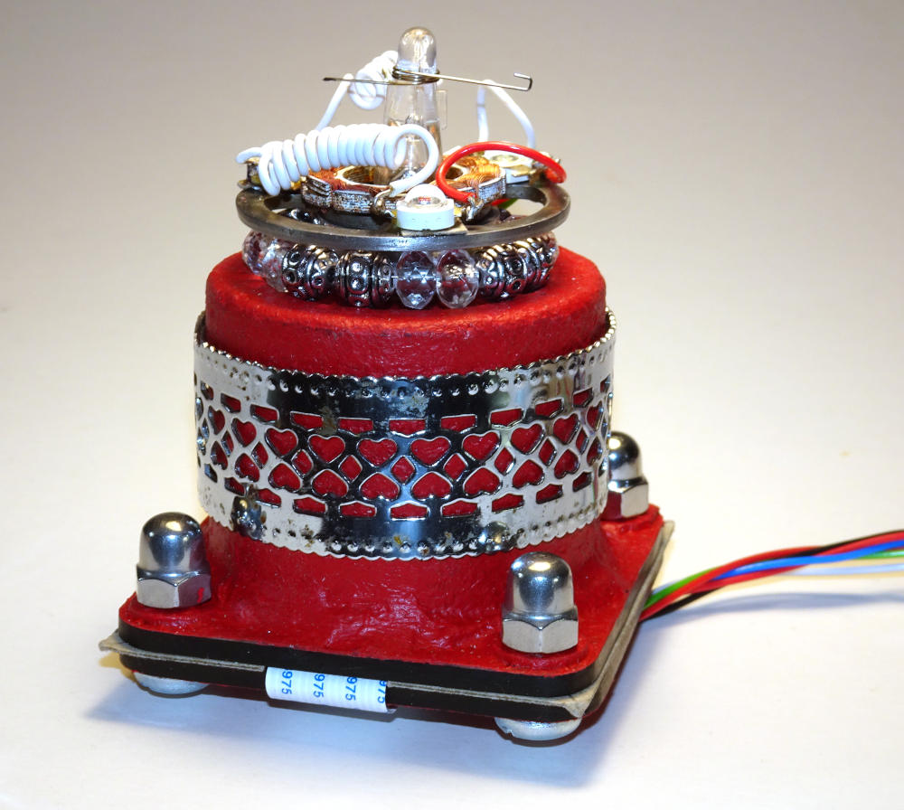
Structural frame
By a combination of stunningly bad pre-planning and overly zealous Steampunking, the main circuitry doesn’t fit through the gap between the rods. They’re simply M6 rods inside ∅6 aluminium tubes (shown with one rod removed):-
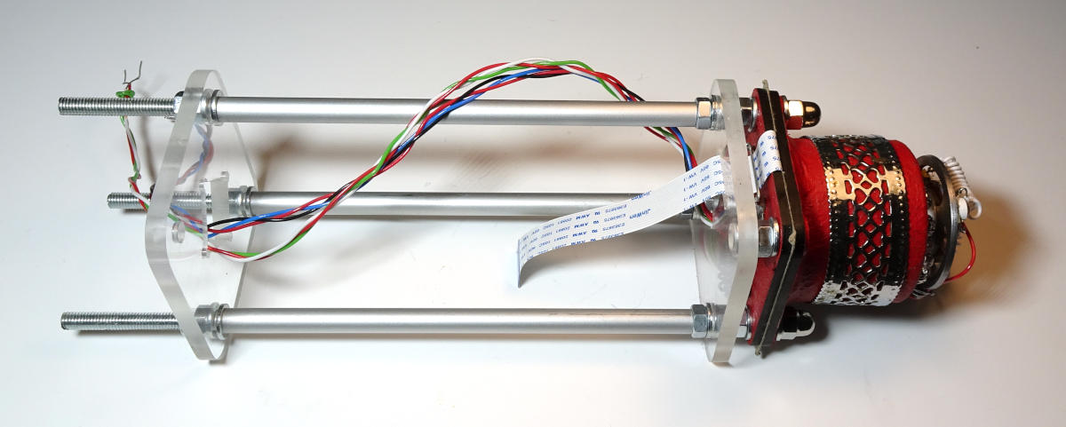
Internal structural frame.
Main circuitry
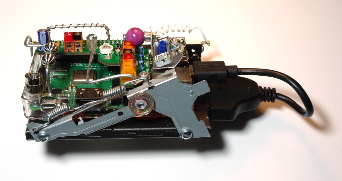
The main circuitry assembly.
The above shows the RPi with the IO PCB plugged in, the SSD below it and some (unnecessary) artistic freedoms. You can just about see the silver Broadcom system chip roughly in the middle of the mess design.
Power PCB
Our mains power is noisy (damn Trevor next door and his plasma cutter) and occasionally suffers brown-outs. So Null Gamma includes a clean up stage that looks like:-
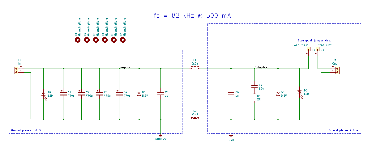
Power PCB schematic.
The main features are bulk capacitance (C1, C2, C3 and C4) and a pi filter (C5, L1, C6 and L2). Cut-off (fc) occurs at 82 KHz under a 500 mA load. It exhibits the characteristic 40 dB /decade roll off. The pi filter is critically damped by a parallel damper consisting of C7 (10μF) and R1 (2Ω), creating a Q of pretty much the ideal 0.7. Otherwise we get an 11 dB gain at 79 kHz. You can see the filter’s frequency performance below:-
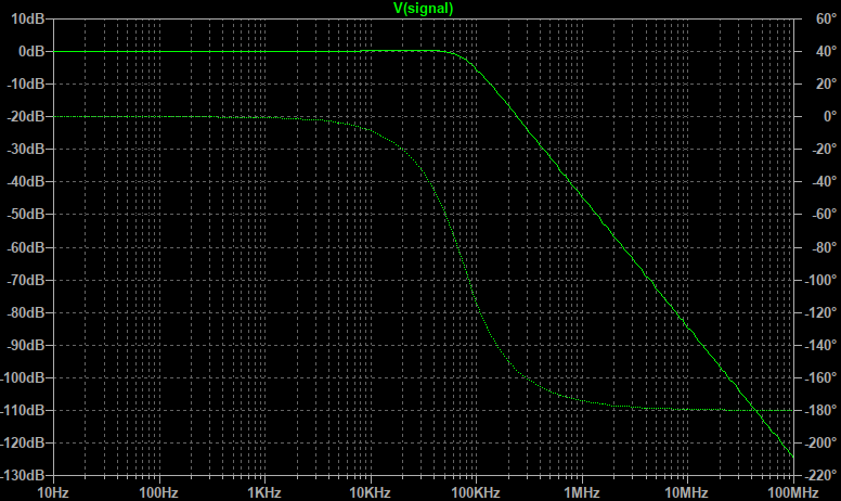
Pi filter response.
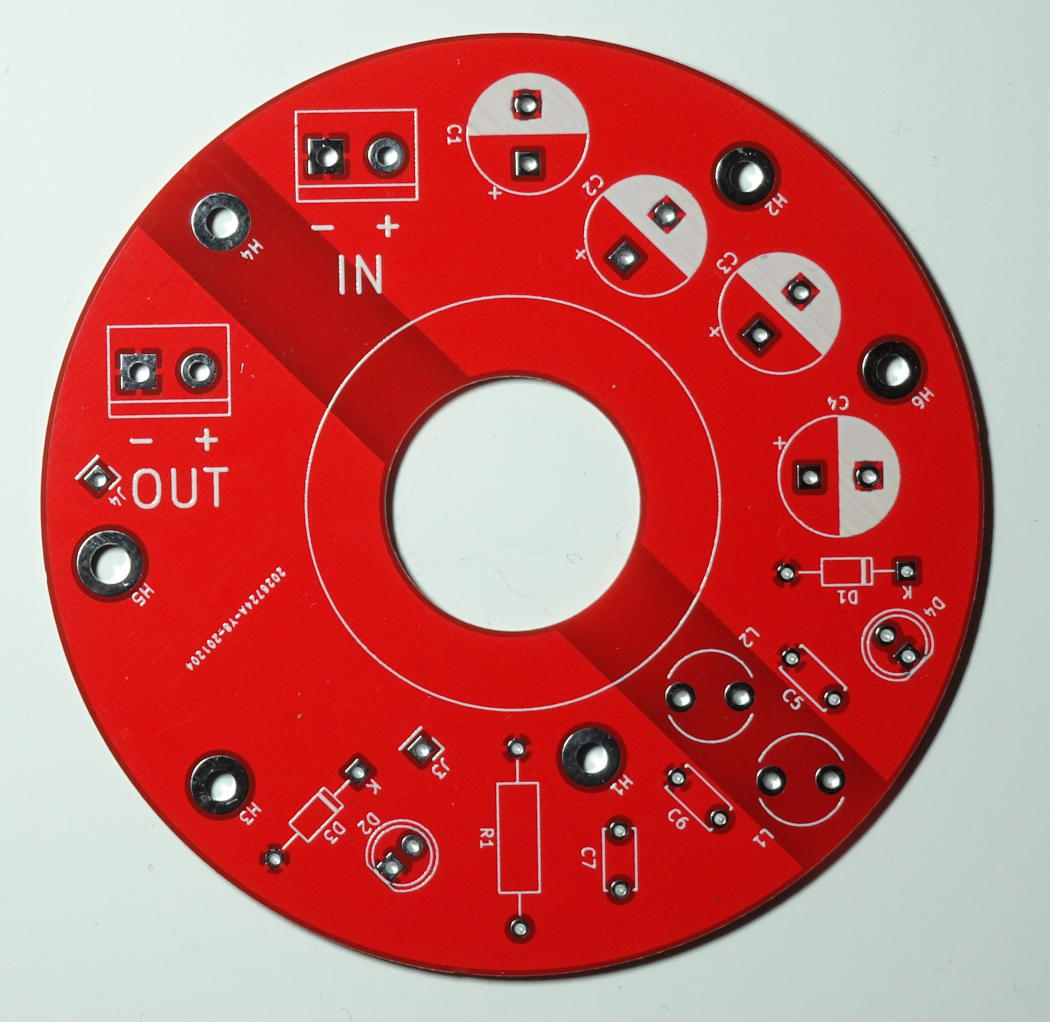
Unpopulated power PCB.
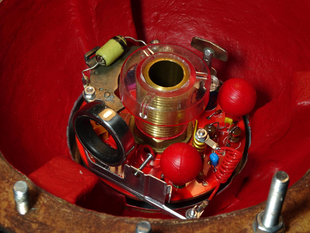
The 45 degree diagonal stripe is the gap between input and output ground planes. The only bridge across them is by the two inductors L1 and L2, both 2.2μH. In situ it looks like (plus minor embellishments):-
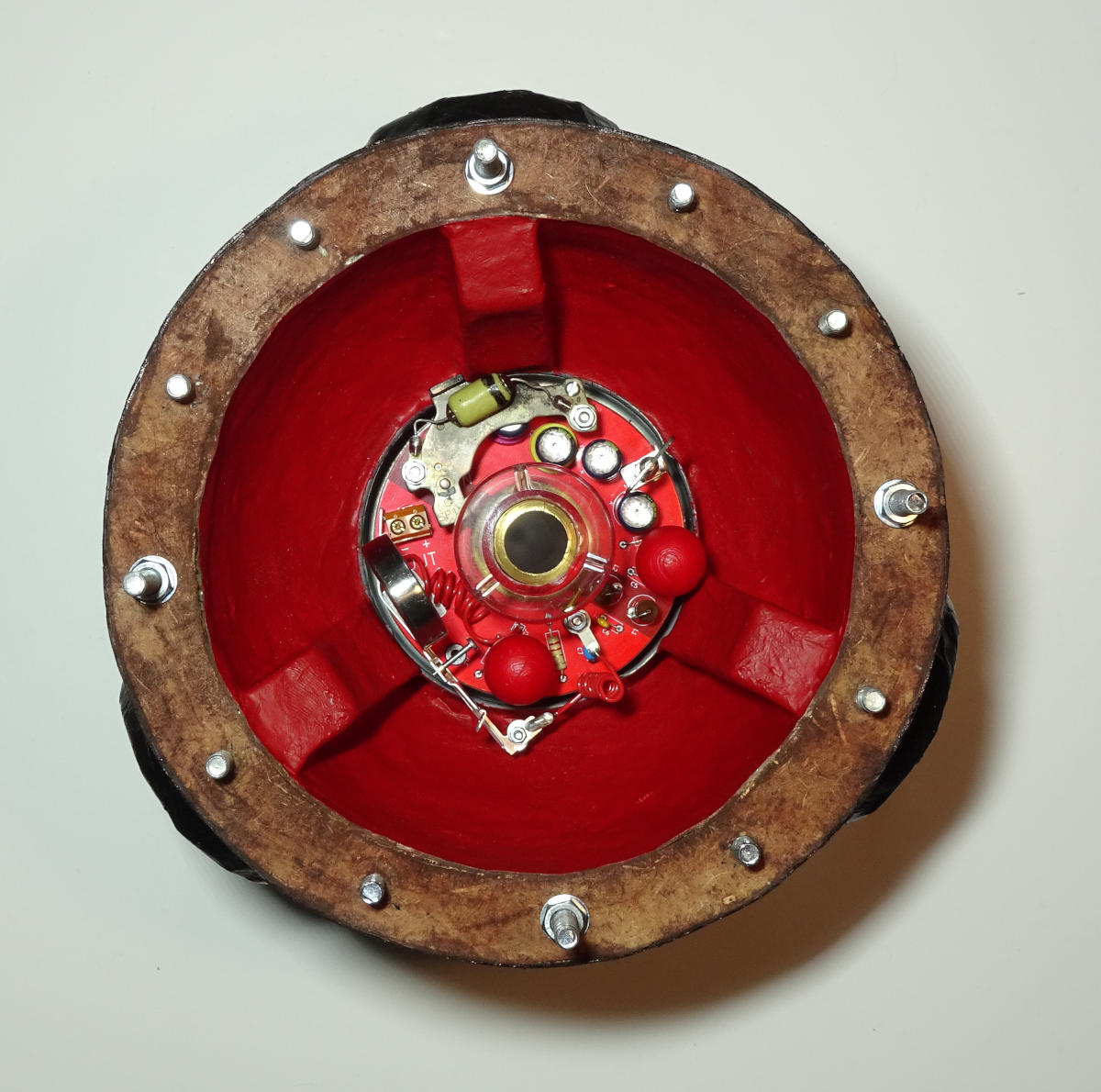
Inside the base hemisphere.
The two 2.2 μH inductors are the vertical brown cylinders situated on the power PCB’s right hand side, between the two red LED balls. Rough (Trevor-grr) 5.1V power and Ethernet connectivity enter the base hemisphere through the central brass entry tube.